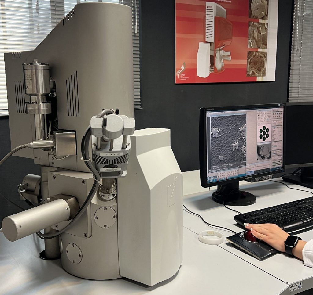
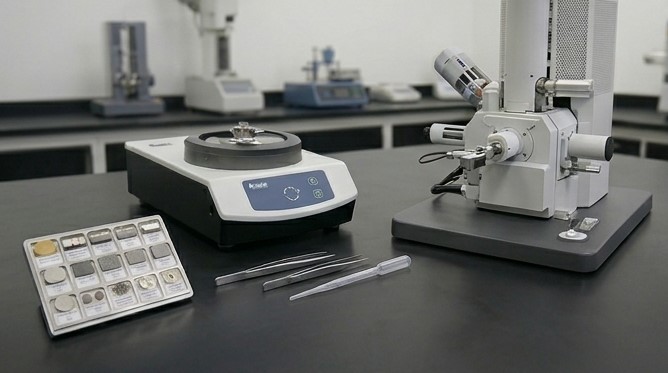
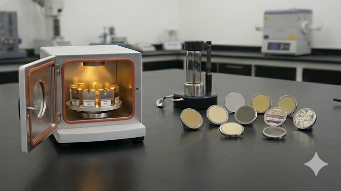
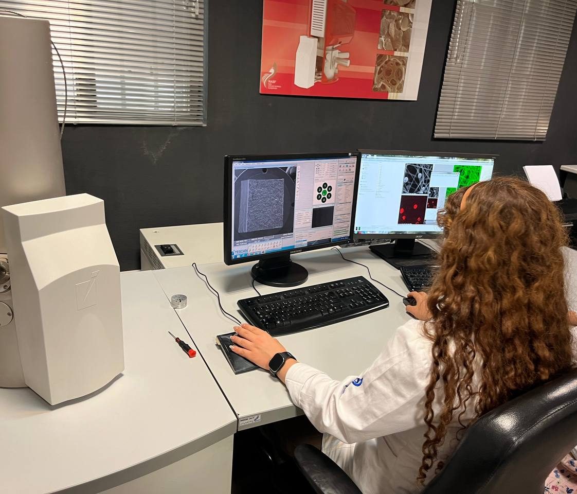
The FE-SEM Laboratory is equipped with a TESCAN MIRA3 Field Emission Scanning Electron Microscope, a versatile platform designed for multipurpose imaging and analytical workflows. The system combines high-current beam stability and In- Beam technology to deliver reliable high-resolution imaging and advanced microstructural characterization.
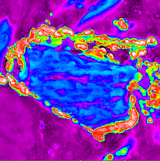
The microscope is equipped with Secondary Electron (SE), Backscattered Electron (BSE), and In-Beam detectors, as well as an Energy Dispersive X-ray Spectroscopy (EDS) analyzer, enabling detailed surface morphology studies, compositional contrast imaging, and elemental analysis.
The TESCAN MIRA3 features an official magnification capability of up to 1,000,000× and allows the investigation of structural features and particles as small as approximately 10 nm. The system is well suited for research and applications in materials science, nanotechnology, geology, electronics, energy, environmental science, and related fields.
 TR
TR