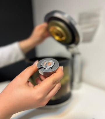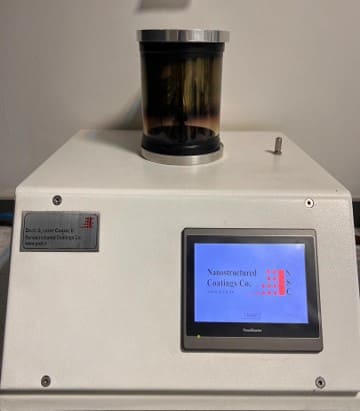


Gold sputter coating is a commonly used sample preparation technique for Scanning Electron Microscopy (SEM). It is applied to non-conductive or poorly conductive samples to improve imaging quality and prevent charging effects during electron beam exposure.
This conductive coating provides several important benefits:
- Prevents electrical charging of non-conductive samples
- Improves electrical conductivity of the surface
- Enhances secondary electron emission
- Increases image stability and resolution
Typical gold coating thickness ranges from 5–10 nm, depending on the application and required resolution.
The thickness of the deposited gold layer on the sample can be accurately controlled by adjusting the parameters of the gold sputter coater.